

Somewhat surprisingly, Nvidia doesn't have much of a track record when it comes to using cutting-edge silicon. But a new report claims that's about to change dramatically, with Nvidia planning to be the very first to use TSMC's next-next gen A16 node.
Taiwanese outlet CTEE claims that Nvidia will be the first to adopt TSMC's A16 node due to competition from AMD, in part for what it calls HPC or high performance chips built on TSMC's upcoming N2 node and due out this year.
The only N2 chips AMD has planned for next year, as far as we know, are server CPUs, not GPUs. AMD's next major AI GPU release, MI450, is expected to be on TSMC N3 silicon.
Nvidia currently uses a version of TSMC's N4 node for all its GPUs. N4 is actually a refinement of N5, which dates back to 2020. Meanwhile, the first chip made on TSMC's N3 technology, the Apple A17 Pro SoC for iPhones, debuted back in 2023.
Consequently, Nvidia is now bumping up against what's known as the reticle limit with its Blackwell generation of GPUs. That's a physical limit on the size of an individual chip that can be etched onto a wafer.
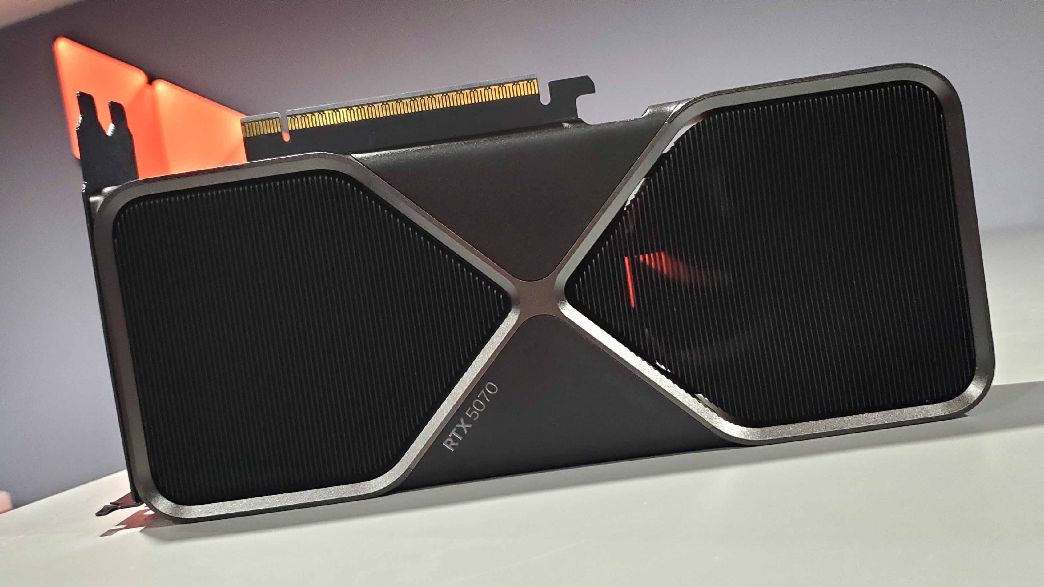
That physical size in turn puts a hard limit on how many transistors can be squeezed into a single chip. Nvidia's most powerful AI GPU, GB200, actually uses a pair of reticle-sized GPUs fused together on a single interposer. Nvidia's RTX 5090 GPU, codenamed GB202, is likewise up pretty close to TSMC's N4 reticle limit at 750mm2.
Indeed, Nvidia essentially carried over N4 production technology from the previous RTX 4090 family to the current RTX 50 GPUs. That's one important reason why the likes of the RTX 5070 and RTX 5080 are barely any better than their direct progenitors.
For Nvidia's next-gen Rubin generation, Nvidia will be using TSMC's N3 node. But if this news about TSMC A16 is correct, Nvidia could skip N2 altogether and jump straight to A16. Of course, the immediate question with all of this is how relevant it is to gaming. The idea that Nvidia might want to accelerate it's AI roadmap onto A16 makes a lot of sense. But gaming GPUs?
The thing is, Nvidia's approach for multiple generations now has been to used a shared GPU architecture across both AI and gaming and produce all chips on the same node. Obviously an AI GPU is very different to a gaming GPU. But certain elements of the chips, such as at least parts of the Tensor cores, are like the same on all chips. That makes it cheaper and faster to engineer GPUn designs for a given node.
Thus, Nvidia's current Blackwell GPUs are all on N4 and its next-gen Rubin GPUs, including both AI and gaming variants, are expected to be on N3. This TSMC A16-related report, if accurate, would apply to the generation after Rubin, which is known as Feynman and is due out in 2028.
If it turns out that Nvidia is indeed skipping N2 and that includes gaming GPUs, too, then it could be very good news. Nvidia will have many more transistors to play with in a couple of generations' time as a consequence. And you'd normally expect that to translate into significantly higher performance and perhaps new features.
Of course, Nvidia also has form for launching disappointingly incremental GPU upgrades, such as Blackwell. But as I said, part of the problem with Blackwell is the old TSMC node. So, this A16 rumour for the Feynman generation could be very positive news for PC gaming. As ever, we'll ultimately have to wait and see.


 Bengali (Bangladesh) ·
  English (United States) ·